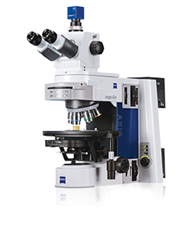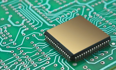
At Allied High Tech Products, Inc., we know that successful outcomes depend on integrated, well-conceived solutions. That's why our focus is on the research, design, manufacture, distribution, service and support of high-quality equipment and consumables for sectioning, mounting, polishing, cleaning, hardness testing, and microscopy and image analysis for companies involved with electrical and physical failure analysis of semiconductor devices.
Allied products are utilized in laboratory and production environments where quality assurance, reliability and failure analysis are used as measures for worldwide compliance and safety.
Because we believe the ability of our customers to effectively use our products is just as important as the effectiveness of the products themselves, we offer comprehensive personalized training and expert technical assistance. And Allied products always offer superior value and are backed by a complete satisfaction guarantee.
With headquarters located in Cerritos, California and a second manufacturing facility in Edmond, Oklahoma, Allied's equipment, consumables and technical expertise are utilized and supported worldwide.
We invite you to investigate the world of Allied High Tech Products.
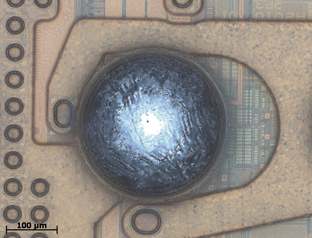
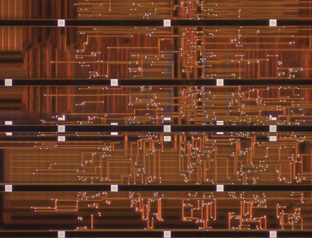
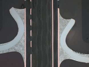
| Solder Ball on Integrated Circuit | Delayered Integrated Circuit | Packages on a PCB |
|---|---|---|
 |
 |
 |
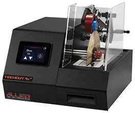
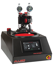
Allied Innovations
Allied's X-Prep® is the most technically advanced instrument of its kind for precision sample preparation. No milling/polishing tool on the market offers similar features & capabilities or produces such accurate results with ease. Now with 3D capability, the X-Prep® allows thinning of non-flat/warped silicon and other substrates with unmatched accuracy. It has been engineered with advanced components and technology to deliver sophisticated, unmatched results and give you exactly what you need in a sample preparation tool.